Fall 2026 · PCB design in progress
SMART
PEN.
A camera board
the width of a pen.
A four-layer, 12 mm-wide board for a pen with a small camera aimed at the page. It has an ESP32-S3, a 5 MP camera, USB-C charging and a Li-Po battery. Two revisions so far; designed and checked, not yet built.
See the board ↓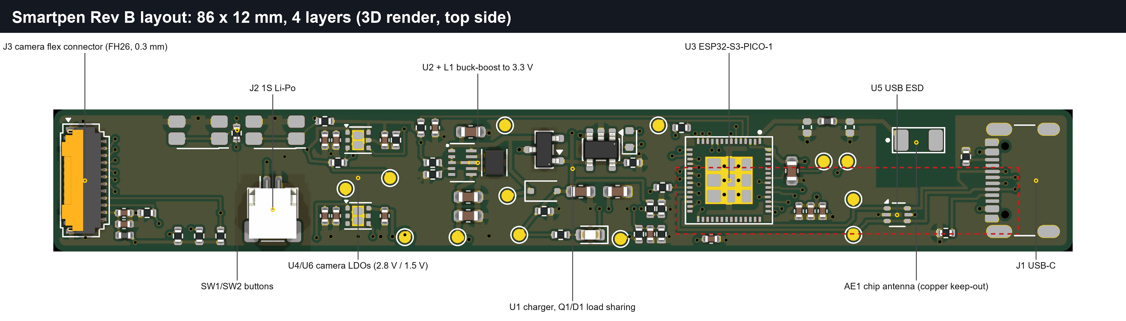
- Status
- Designed and checked · not yet fabricated
- Board
- 86 × 12 mm · 4 layers
- Key parts
- ESP32-S3 · OV5640 · MCP73831 · TPS63802
- Tools
- KiCad 10
Schematic to layout
The board.
86 × 12 mm, four layers. Camera connector on the left, ESP32-S3 in the middle, USB-C and the chip antenna on the right.
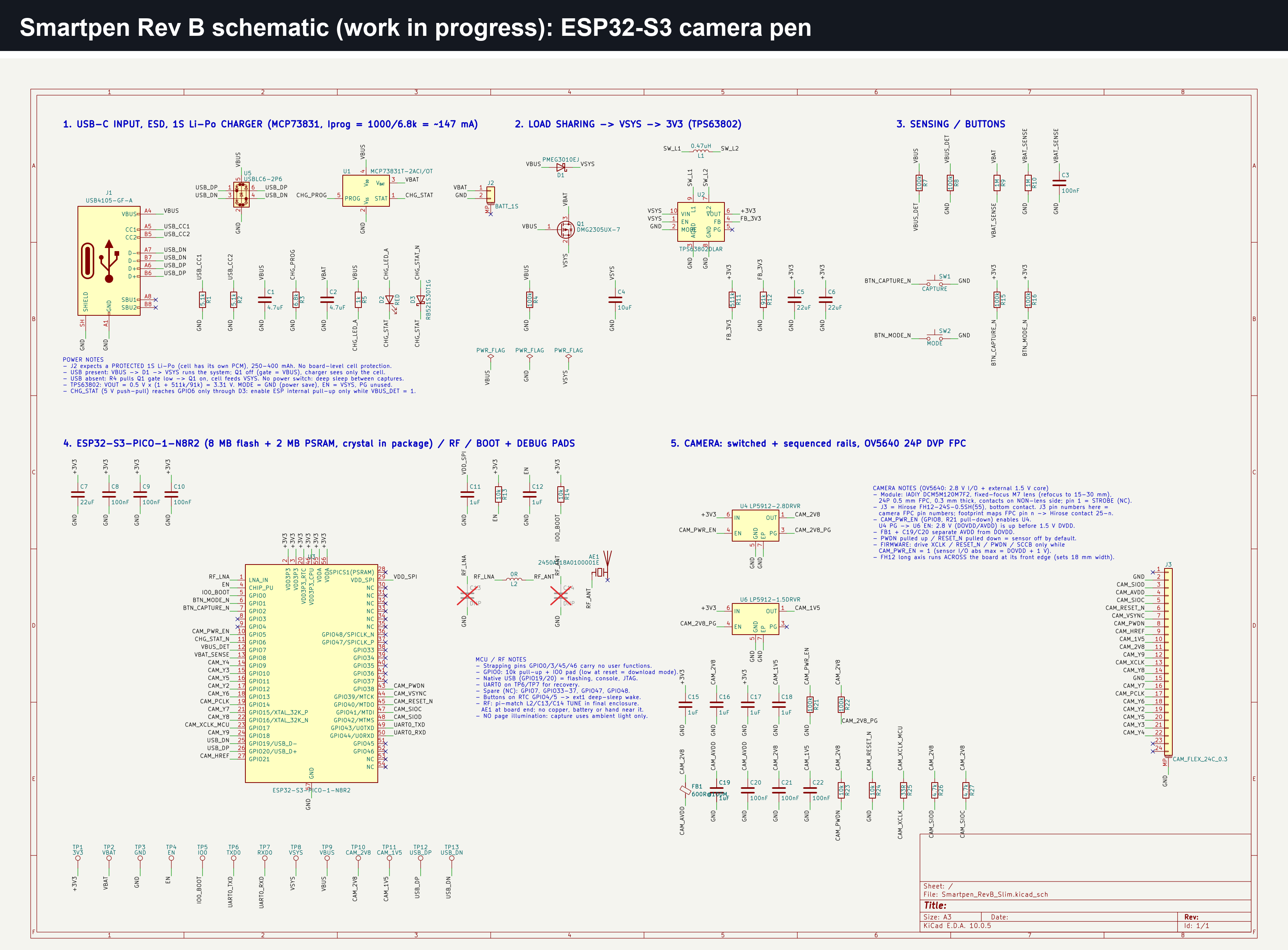
Five blocks: USB-C input and charging, power path and 3.3 V, buttons and sensing, the ESP32-S3 with its antenna, and the camera rails.
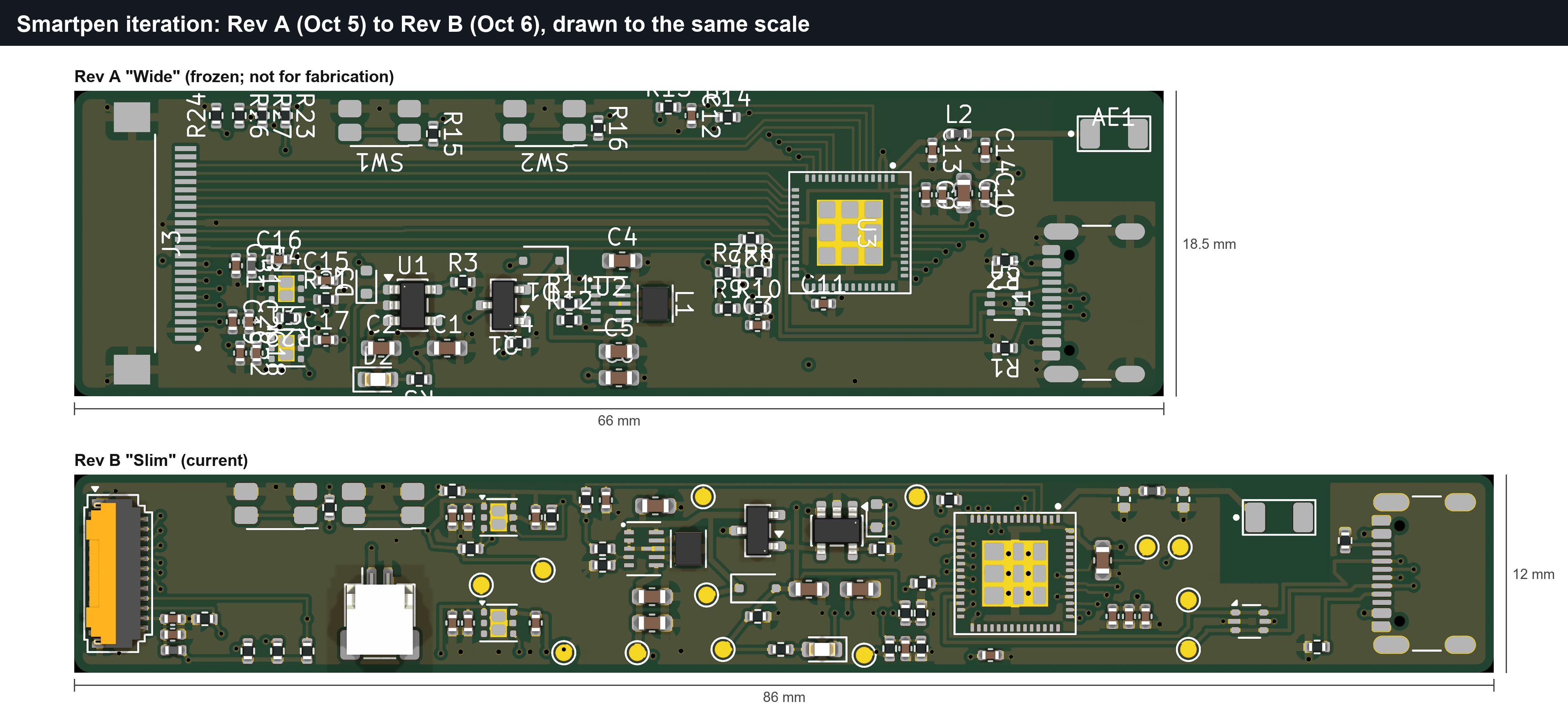
Both revisions drawn to the same scale. Rev A was 18.5 mm wide. Rev B is 12 mm wide and 20 mm longer.
Start with the width
A pen is only about a centimeter across, so the width of the board is the number everything else has to fit inside. In Rev A, the camera’s connector lay across the board: 24 contacts at a 0.5 mm pitch, plus the housing. That one part set the board at 18.5 mm wide. Too fat to hold like a pen.
So Rev B changes the connector, not the layout around it. A 0.3 mm-pitch connector with a custom flex cable shrinks that edge, and moving every part onto one side freed up the rest. The board went from 18.5 mm to 12 mm wide. The cost was length: it grew 20 mm, partly to fan out the camera’s two rows of contacts.
Power, from the battery up
It runs on a small protected 1S Li-Po (250–400 mAh) and charges over USB-C through an MCP73831. One resistor sets the charge current: 1000 V ÷ 6.8 kΩ ≈ 147 mA. That keeps even the smallest cell well under 1C, so charging stays gentle.
When USB is plugged in, the board runs straight from USB through a diode and a transistor cuts the battery out of the load. That way the charger only ever sees the cell, so it can tell when the cell is actually full. When USB is unplugged, the transistor turns on and the battery takes over.
A Li-Po sits anywhere between about 4.2 V full and 3.0 V empty, and the ESP32 wants 3.3 V. That’s above 3.3 V for part of the discharge and below it for the rest, so a regulator that can only step down isn’t enough. The TPS63802 buck-boost does both. Its divider sets the output: 0.5 V × (1 + 511k ÷ 91k) ≈ 3.31 V.
There’s no power switch. The ESP32 sits in deep sleep between captures, and the two buttons are on pins that can wake it up.
The camera wants its power in order
The OV5640 camera needs 2.8 V for its I/O and analog side and 1.5 V for its core, and the 2.8 V has to come up first. So the 2.8 V regulator’s “power good” output is what enables the 1.5 V regulator. The order is set by the hardware, not by firmware timing.
Both regulators hang off one enable pin, so the camera can be switched off completely when it isn’t taking a picture. A ferrite bead and capacitors keep the analog supply separate from the noisier I/O supply. The camera’s I/O pins can only handle 1 V above its own supply, so the firmware rule is simple: never drive the camera’s clock, reset or control lines unless the camera is powered.
The lens is a fixed-focus module refocused to 15–30 mm, close enough to see the page under the pen. There’s no light on the board, so it captures with whatever light is in the room.
Four layers, one job each
Top: the parts, USB and the antenna feed. Inner layer 1: a solid ground plane, so every fast signal on top has its return path right underneath it. Inner layer 2: the camera’s parallel data bus and power links. Bottom: buttons, status lines and the main power traces.
The chip antenna sits at the very end of the board with no copper, battery or hand near it, and the ground pours are cut back around it. Copper next to an antenna detunes it. A small matching network next to the antenna is left to tune once it’s in its final case.
What Rev B fixed, and what it broke
Rev B cleared every silkscreen, annular-ring, hole-clearance, thermal-relief and footprint problem from Rev A, and the schematic and board now match exactly.
| Rev A · Oct 5 | Rev B · Oct 6 | |
|---|---|---|
| Board | 66 × 18.5 mm, 4 layers | 86 × 12 mm, 4 layers |
| Camera connector | Hirose FH12, 0.5 mm pitch, across the board | Hirose FH26, 0.3 mm pitch, plus a custom 24-conductor flex |
| Parts | Both sides | All on the top side |
| Design-rule check | 256 issues | 18 issues (17 on the USB pair) |
| Schematic vs. board | 76 mismatches | 0 |
| Electrical rule check | 0 errors | 0 errors |
The 17 remaining issues are all the USB data pair, against a rule I set myself. In Rev B the ESP32 sits about 26 mm from the USB-C connector instead of 16 mm, and a 12 mm-wide board leaves little room to keep the two lines side by side. The pair separates by up to 5.9 mm (my limit is 0.18 mm) and runs 17.2 mm uncoupled (my limit is 3 mm). The ESP32-S3’s USB runs at full speed, 12 Mbit/s, which is far less sensitive to this than high-speed USB. I haven’t analysed or tested it yet, though, so it stays open.
What’s next
Fix the USB routing, either by moving the ESP32 closer to the connector or by rerouting the pair. Check the camera flex pinout against the module datasheet one more time; the camera notes still describe the Rev A connector. Then order boards.
Bring-up will go one layer at a time: power the board without the camera and check every rail first, then measure current in sleep and awake, then plug in the camera. If something is wrong, I want to find it before it can damage the part I can’t easily replace.
Right now this is a design: laid out and checked, but not built or tested.
Explore more of the work.
← Back to Selected Builds