Experiments in Physics · Cleanroom
Graphene Transfer
Moving a layer one atom thick without wrecking it, then checking what actually survived.
Explore the engineering ↓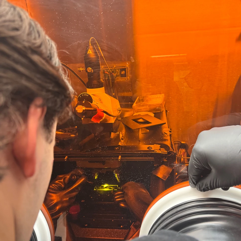
- My role
- Lab work and presentation, with my lab partner Hunter
- Status
- Samples transferred and measured
- Focus
- Wet transfer · Raman · AFM
What we found
After the transfer, Raman showed the G (~1580 cm⁻¹) and 2D (~2700 cm⁻¹) peaks you expect from graphene. What it couldn’t tell us is how many layers we had or how clean the transfer was.
- 01
Support
Coat the graphene on copper with PMMA so it has something to hold it together.
- 02
Transfer
Etch the copper away and float the film onto a new substrate.
- 03
Locate
Use contrast under the microscope to pick where to look.
- 04
Characterize
Check those spots with Raman, and the flakes’ height with AFM.
In the lab
Inside the work.
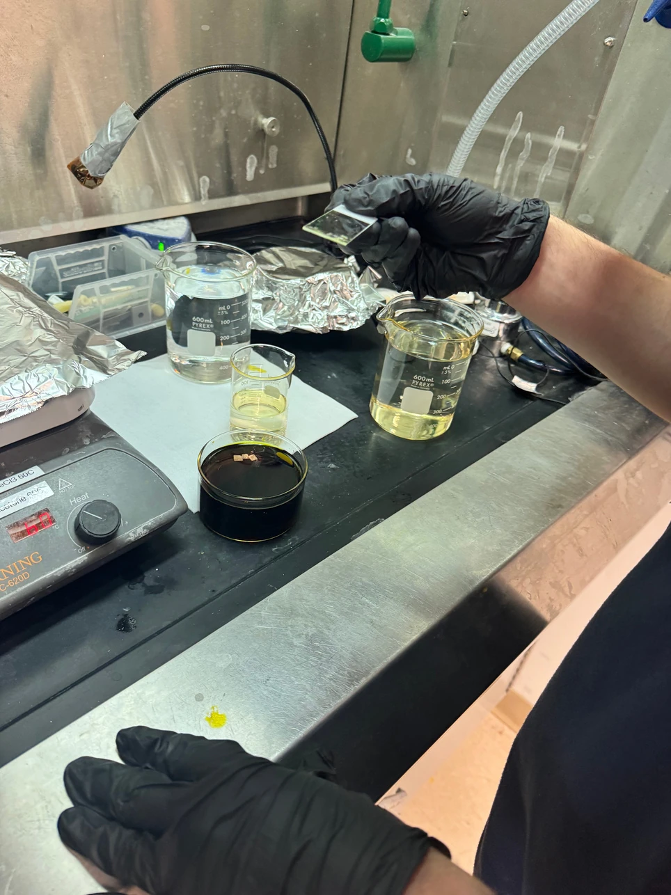
Taking the samples through the wet steps. This is where the film is most likely to tear.
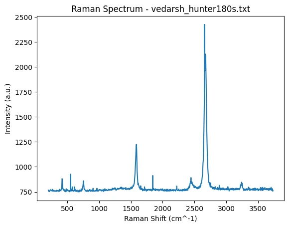
The G and 2D peaks from our transferred film.
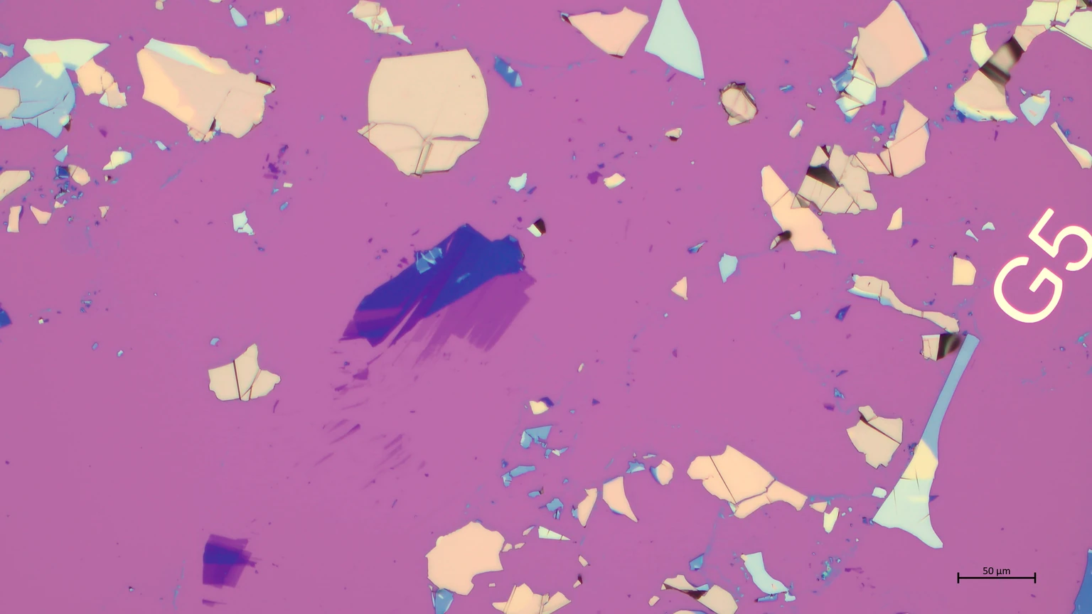
Flakes vary a lot in size and contrast, so we measured them one region at a time.
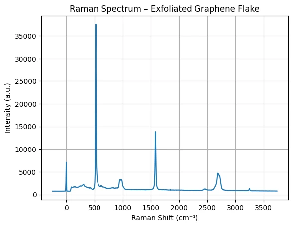
This one also shows a D peak near 1350 cm⁻¹, a sign of defects.
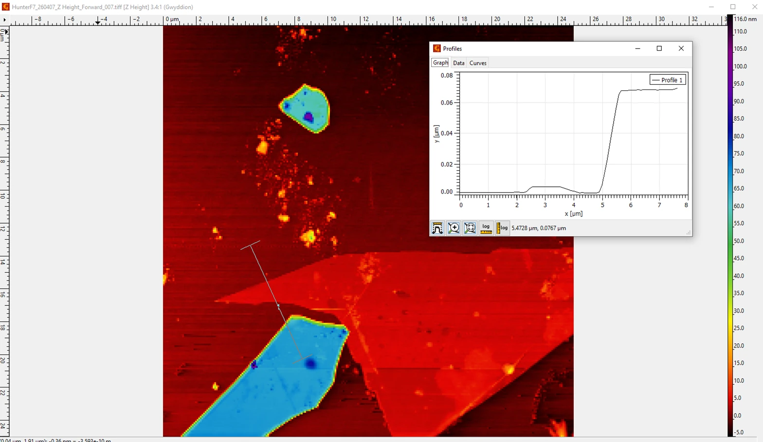
The height step at a flake’s edge. It shows layers, but not that it’s a single layer everywhere.
Two ways to get graphene
We worked with two kinds of sample. CVD graphene grows as a continuous sheet on copper, so the hard part is moving it without breaking it. Exfoliated graphene is peeled off graphite with tape, which gives cleaner flakes but random sizes and thicknesses. They answer different questions, so we kept them separate.
Moving a film one atom thick
You can’t pick up a single layer of atoms, so we gave it a backbone first: a thin PMMA coating. Then the copper underneath is etched away, the PMMA-and-graphene film floats free, and we scoop it onto a new substrate. After that, the PMMA comes off and we check what’s left.
Two instruments, two questions
Raman tells you what the material is. Graphene has a G peak near 1580 cm⁻¹ and a 2D peak near 2700 cm⁻¹, and a D peak near 1350 cm⁻¹ shows up when there are defects. AFM tells you its shape: a sharp tip dragged across the surface measures height, so a flake’s edge shows up as a step. We used the microscope to choose spots and both instruments to look at them.
What we can and can’t claim
The transferred film shows the graphene peaks, and the flakes show a layered step. That’s good evidence we had graphene. It doesn’t tell us we had a single layer everywhere, how many defects there were, or how much of the film survived. Our flakes were uneven, and some were probably several layers thick.
Sources
Technical records.
Continue exploring.
← Back to Selected Builds